This is the week where we started actually making our own PCB boards, if theres any faults with the board now, its our own fault as its our own design.. We didnt have to worry about the LCD board not working, as that was given to us so we knew it worked, I suppose I had to trust Ray on this one 😀
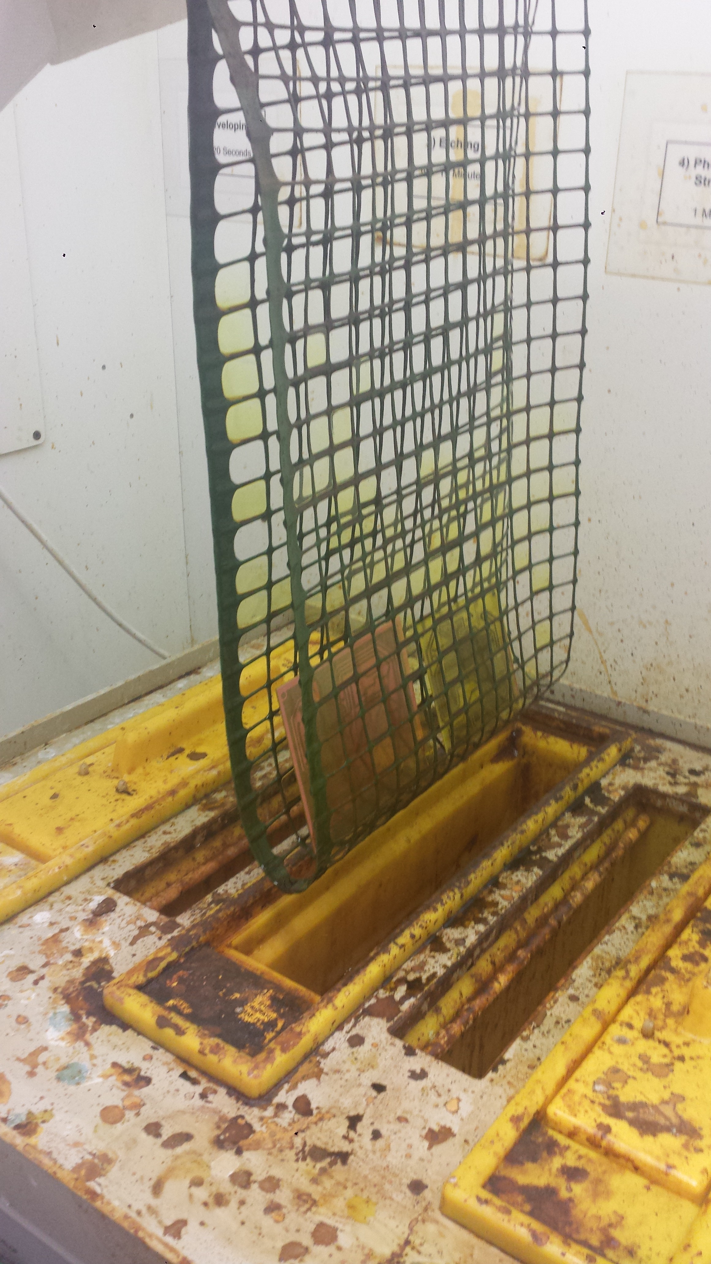
The Manufacture of the sensor and control board involved a number of steps. First of all, I had to print the artwork that would be put onto some one sided fibreglass PCB board, peeled the protective layer off the PCB, and then put it in the sealed UV light machine to print the artwork onto the physical board. When this was done, the board was then put into a number of tanks.
Tank 1:
Developing – this tank removes the UV sensitive chemicals from the board. This will leave something like a stencil on the board thats in the shape of my original design.
Tank 2:
Etching – This tank removes the copper wherever the ‘stencil’ isint protecting it. After this process is done, we can now see all the different electrical connections that make the circuit.
Tank 3:
Photoresist Stripping – The photo resist is now removed off the copper tracks that are on the board.
Tank 4:
Tinning – Because copper tracks are now visible, a protective layer has to be put on the copper tracks otherwise they would oxidise, making them unusable.
Board in process of being manufactured
Next was assembly of the boards, placing the components and soldering them into the correct spot for them. Because this was such a time consuming thing to do, it took both weeks 4 and 5 to do, but I didnt mind because I wanted it to work correctly the first time so did not want to rush it.
